| Poster Number |
Poster Authors |
Affiliation |
Title |
Abstract |
PDF |
| 1 |
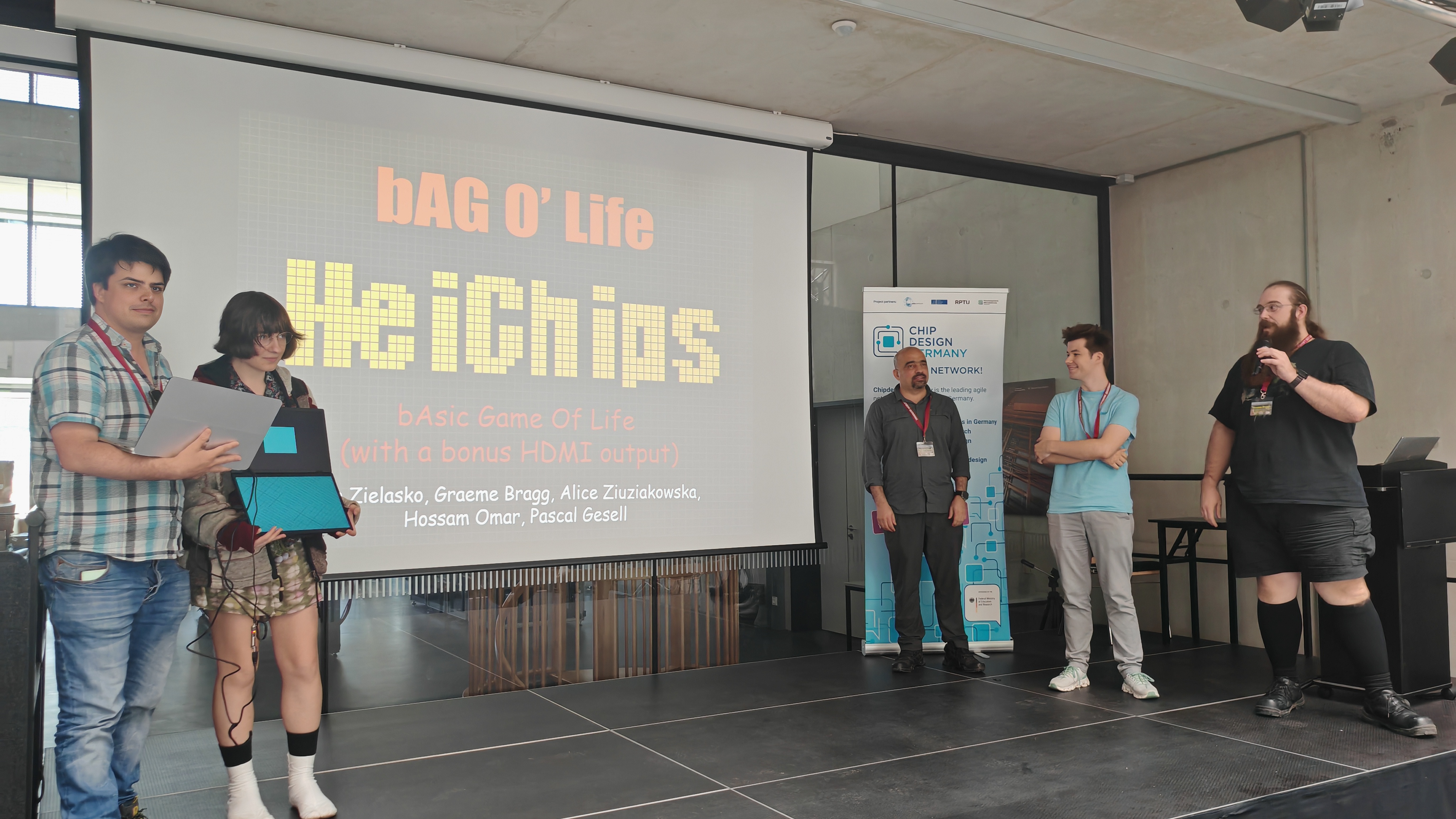
Pascal Gesell |
Bern University of Applied Sciences |
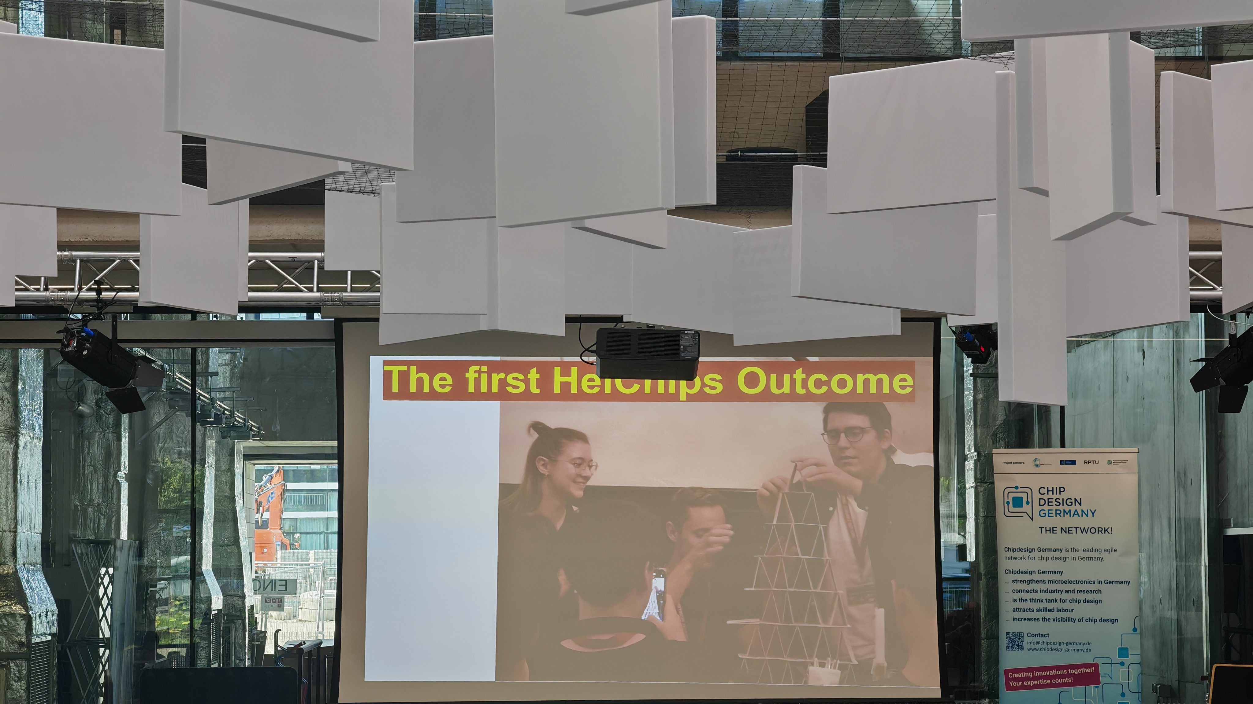
Ever wanted to design your own ASIC in VHDL? |
This project investigates the implementation of a digital storage oscilloscope (DSO) on an application-specific integrated circuit (ASIC) using Tiny Tapeout. By employing modular design and open-source tools, it addresses challenges such as limited on chip memory and the specific constraints of ASIC design. The outcome demonstrates the feasibility of compact and functional ASIC development, integrating features like video output, external F-RAM buffering, and a test signal generator. |
PDF |
| 2 |
Graeme M. Bragg, Jules Field |
University of Southampton |
Moodle & Verilator make open-source, web-based automated marking of SystemVerilog labs a reality |
Moodle & Verilator make open-source, web-based automated marking of SystemVerilog labs a reality |
PDF |
| 3 |
Marcin Kowalczyk |
AGH University of Krakow |
Processing event data from a neuromorphic vision sensor |
Event cameras are neuromorphic sensors inspired by the human visual system. Due to the format of the vision data being sent, it is necessary to develop new algorithms and hardware archiectures to process it efficiently. |
PDF |
| 4 |
Varun Posimsetty |
Technical University of Munich |
Low Cost Power Cycling Stimuli Generator for AMS Validation using an FPGA |
A cost-effective, low-latency FPGA-based power cycling stimuli generator for post-silicon validation of analog mixed-signal devices. Traditional validation setups suffer from high equipment costs and switching delays. The proposed system replaces expensive multi-channel signal generators with a scalable FPGA solution capable of generating synchronized digital pulses and analog ramps. |
PDF |
| 5 |
Spandan Das, Christoph Lueth, Tim Gueneysu, Pascal Sasdrich, Rolf Drechsler |
University of Bremen and Ruhr University Bochum |
EMBOSOM
Emigrating Embedded Software Security into Modern Emerging Hardware Paradigms |
Embedded systems are the basic building blocks of complex electronic devices and as such, their security must be guaranteed to ensure safety of the device itself. For such systems, it is very difficult to install additional software level security on top of the main program because of the space crunch. Hence our approach is to design a secure hardware along with an Instruction Set Architecture (ISA) such that the software becomes inherently
secure in memory, even when designed using a fundamentally memory-unsafe programming language like C or C++. In order to achieve this, we are implementing a tagged memory along with an extended RISC-V ISA (an approach similar to CHERI) on an existing RISC-V Virtual Prototype, that can simulate the behavior of memory starved embedded systems. |
PDF |
| 6 |
andrea.quirini, aisha.baloch, fabia.arshad, fabiola.colone, pierfrancesco.lombardo}@uniroma1.it |
Ph.D researcher |
Radar Frequency-Comparison Monopulse Validation Using FPGA-Generated Wideband Chirp Waveforms |
Abstract: In this paper, we introduce a frequency-based Direction of Arrival (DoA) estimation technique for wideband radar systems employing Linear Frequency Modulated (LFM) signals. Conventional phase-comparison monopulse is subject to estimation ambiguities, especially in the case of a large baseline distance. In contrast, the proposed frequency-comparison monopulse leverages the time-to-frequency mapping property of LFM signals, enabling unambiguous DoA estimation for any antenna spacing. By leveraging a fully digital generation method for LFM signals implemented on the ZCU111 FPGA platform, we carry out an validation test of the frequency-comparison monopulse, demonstrating its effectiveness in addressing the limitations of conventional monopulse |
PDF |
| 7 |
Gulafshan |
Universtät Heidelberg |
MemSim+: Realistic Behavioral Model for ReRAMs Capturing Non-Idealities |
Memristors are promising candidates for in-memory computing systems, offering a potential solution to the von
Neumann bottleneck in traditional computing architectures. Designing reliable and efficient memristive circuits re-
quires accurate simulation models that can reflect real-world device behaviors, including their inherent non-idealities.
In this talk, I will present MemSim+[1], a comprehensive behavioral model for memristors that captures both cycle-to-
cycle (C2C) and device-to-device (D2D) variations in key parameters, such as high and low resistance states, threshold
voltages, resistance drift, and switching dynamics. Unlike traditional models that rely on fixed values of key parameters
[2,3,4,5,6], MemSim+ accounts for statistical distributions of these parameters—derived from extensive experimental
data—to emulate real device variability. The model’s universality is validated using two types of memristors: SDC
(Self-Directed Channel) and ECM (Electrochemical Metallization) devices. Electrical characterization was conducted
on different SDC and ECM devices to capture D2D variability, while repeated measurements were performed on one
device of corresponding technology to capture C2C variations. To more accurately emulate real-world non-idealities
in memristor behavior, MemSim+ employs clipped Gaussian and multi-Gaussian approaches—going beyond the tra-
ditional use of simple Gaussian distributions. These advanced statistical fitting techniques allow the exclusion of
critical outlier ranges and provide a more accurate representation of key parameter variations. As a result, the Mem-
Sim+ model captures the full spectrum of device variability more effectively, including memristance, resistance drift,
threshold voltage, and switching dynamics.
To demonstrate the impact of this variation-aware modeling, MemSim+ was used in circuit-level simulations of two
stateful logics: IMPLY logic and FELIX-OR logic. The design constraints of these circuits depend on technological
parameters as well as non-idealities of the memristor in that technology. Hence, a variation-aware circuit-technology
co-design is crucial for maximizing the correct functionality of conceptual circuits. As the result, variation-aware
circuit-technology co-design can significantly enhance the correctness probabilities of the IMPLY logic gate circuit,
achieving correctness probability up to 88.75% (↑ 3.00%) for SDC technology and 85.75% (↑ 4.25%) for the ECM
technology. Additionally, for the FELIX OR gate, the correctness probabilities increase to 85.75% (↑ 35.25%) for SDC
technology and 84.00% (↑ 10.50%) for the ECM technology. The findings indicate that the typical simulation approach
(using nominal values) leads to lower chances of the fabricated circuits functioning as expected. The results showcase
the significance of circuit-technology co-design and their co-dependence, as well as the importance of considering
non-idealities in the behavior of real devices when designing memristive circuits and systems. |
PDF |
| 8 |
Can Joshua Lehmann, Lars Bauer, Hassan Nassar, Heba Khdr, Jörg Henkel |
Karlsruhe Institute of Technology |
Hardware/Software Co-Analysis for Worst Case Execution Time Bounds |
We present a novel method for computing worst case execution time bounds without using a preexisting timing model. Instead, our method computes the WCET bound based on an instrumented hardware description of the target processor. This enables our method to automatically analyse a program's timing behavior in the presence of custom instruction set extensions. |
PDF |
| 9 |
Emmanuel Innocent and Dr. O. O. Ilori |
Obafemi Awolowo University, Ile-Ife Nigeria |
A Highly Linear Wide Bandwidth Programmable Gain Amplifier in 0.18μm CMOS Process |
Programmable Gain Amplifiers (PGAs) are fundamental to optimising signal dynamic range in systems such as medical electronic devices, telecommunications, and disk drives. In automatic gain control (AGC) systems, PGAs help maintain consistent signal levels under varying signal strengths, requiring a wide dB-in-linear gain range. However, modern analogue front-ends demand not only wide gain control but also high bandwidth, low power consumption, compact area, and good noise performance.
This project presents the design of a CMOS PGA targeting a gain range of –12 dB to 20 dB, bandwidth of 100–500 MHz, distortion ≤ –55 dB, and power consumption ≤ 25 mW. The initial implementation uses an operational transconductance amplifier (OTA) with series and feedback switch-resistor networks. Both conventional folded cascode (FC) and recycling folded cascode (RFC) amplifiers were explored. While the RFC provided improved open-loop gain and gain-bandwidth product over the FC, the closed-loop bandwidth remained limited to 1–2 MHz — far below the target.
The current implementation achieved a figure of merit (FoM) of 1187 MHz·pF/mA, and closed-loop bandwidth was extended by a factor of 100 due to feedback. However, redesign is needed to meet the bandwidth requirement. Future work proposes a current operational amplifier based on the second-generation current conveyor (CCII), leveraging current-mode techniques to achieve high speed and low power operation. This approach, when implemented with high-speed IHP BiCMOS technology, is expected to meet the performance targets for wideband, low-power PGAs in modern systems. |
PDF |
| 10 |
Jan Zielasko, Rolf Drechsler |
Institute of Computer Science, University of Bremen, Germany
Cyber-Physical Systems, DFKI GmbH, Germany |
Optimizing Hardware for Neural Network Inference using Virtual Prototypes |
This poster shows how virtual prototypes can be used as an analysis platform to identify suitable application specific hardware optimizations. |
PDF |
| 11 |
Jonas Bühler, Arun Ashok, Lammert Duipmans, Christian Grewing, Dennis Nielinger, Patrick Vliex, André Zambanini, and Stefan Van Waasen |
Institute for Integrated Computing Architectures (ICA) – PGI-4, Forschungszentrum Jülich GmbH, Germany |
TOWARDS SCALABLE READOUT IC‘S
FOR SEMICONDUCTOR QUANTUM DOTS |
Universal quantum computing requires a scalable system with millions of qubits.
Realizing fast, high-fidelity readout remains a central bottleneck, particularly when
striving for scalable architectures that minimize spatial overhead, wiring density, and
energy consumption. To address these limitations, we present our activities on
development of integrated circuits at cryogenic temperatures. Especially an integrated readout circuitry implemented in a 22 nm FD-SOI technology. This IC will be connected to a Single Electron Transistor (SET). The prototype is made for reading out two SETs. It implements a high-speed mode for single-bit readout, enabling rapid discrimination between
the│0〉and │1〉state, as well as a high-resolution mode for tuning, which amplifies the signal and passes it to the room-temperature electronics. We characterize this IC inside a closed cycle Gifford-McMahon cryostat at a temperature of 6 K. The measurement shows a power consumption of 33.6 μW/SET for the single-bit readout and 216 μW for the high-resolution mode. With the correlated double sampling with times of 2×1 μs, the circuit shows low noise of 223 pA (1σ) for single-bit readout, while the high-resolution mode has an input-referred noise level of 188 pA RMS (10 Hz to 1 MHz).
The IC advances scalable, integrated readout solutions and marks a critical milestone on the path toward universal quantum computing |
PDF |
| 12 |
Luis E. Ardila-Perez, Lukas Scheller |
Karlsruhe Institute of Technology (KIT) |
SCALLOP: A Scalable CryoCMOS DAC Array in IHP 130nm BiCMOS for Flux-Bias Control of Superconducting Qubits |
Superconducting qubits are one of the most promising technologies for building large-scale quantum computers. However, scaling these systems from a few qubits to thousands or more requires a fundamental rethinking of how we control them, especially when it comes to delivering precise magnetic flux to each qubit.
Today, this is typically done using room-temperature DACs that generate analog signals routed through long, lossy cables into the cryostat. This approach is not scalable. The flux DACs quickly become the limiting factor, consuming too much power, space, and wiring bandwidth as the qubit count increases.
SCALLOP focuses on solving this problem first, by designing low-power, high-precision DACs and associated sequencer logic that operate directly at cryogenic temperatures (~4K), close to the qubits themselves. To make this possible, SCALLOP uses a fully open-source ASIC design flow, making the development transparent, collaborative, and accessible. These DACs are being developed using the new cryo-compatible PDK from IHP, a BiCMOS process specially tailored for operation at low temperatures and high frequencies, ideal for integration with superconducting qubit systems. |
PDF |
| 13 |
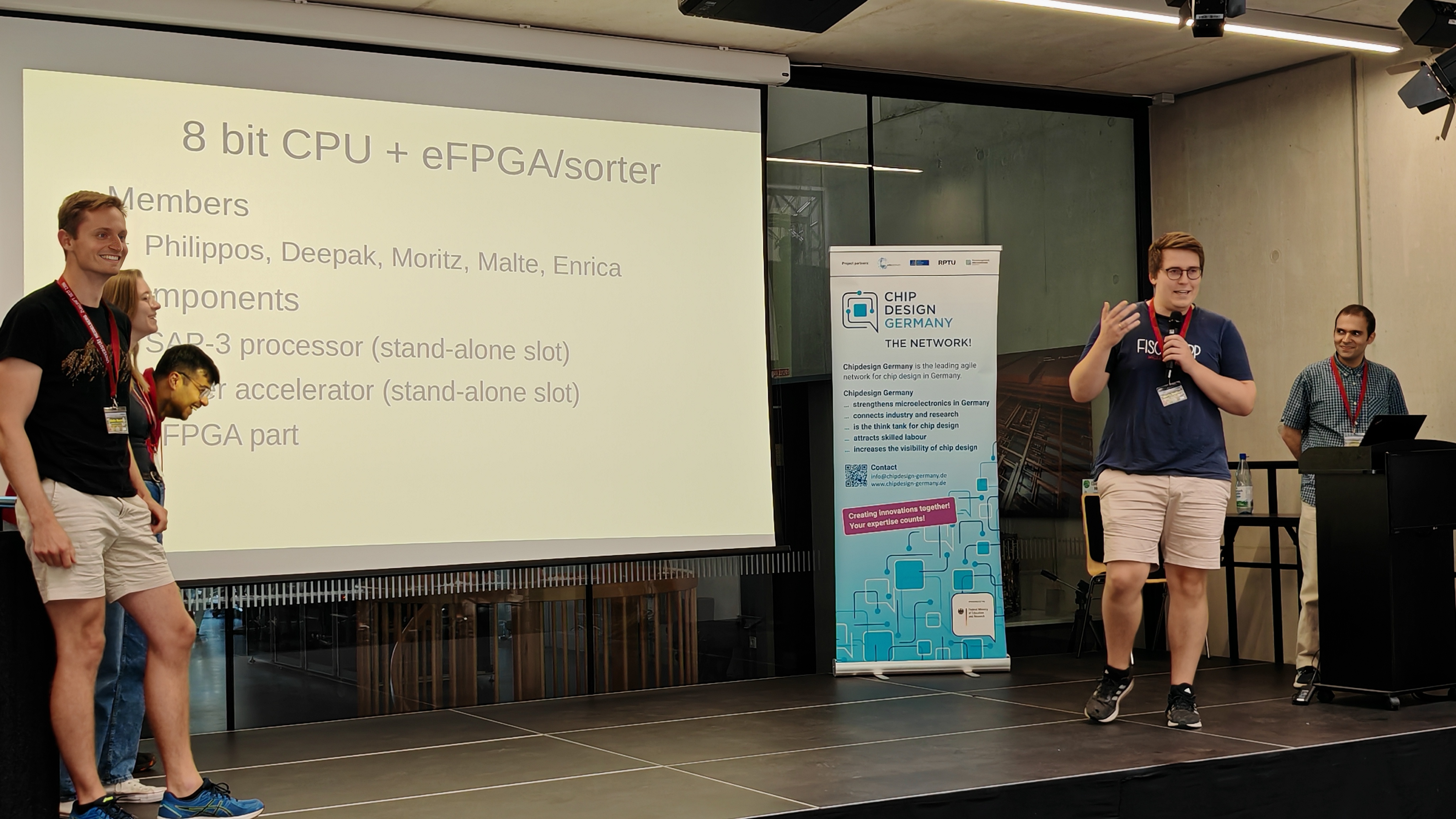
Philippos Papaphilippou |
University of Southampton |
Reconfigurable processing units inside RISC-V cores |
This poster discusses the possibility to integrate small FPGAs inside CPU cores. A general purpose architecture that includes FPGAs has already been introduced to combine the advantages of FPGAs and CPUs, such as flexibility and easy development. The goal is to increase the homogeneity of eFPGA-based solutions within the rest of the core architecture, such as for RISC-V cores, so that the remainder of the micro-architecture evolves in unison with the added reconfigurability. Ongoing research investigates how to best "connect" the two technologies, with the help of the increasingly open nature of RISC-V and eFPGAs. |
PDF |
| 14 |
Hossam O. Ahmed |
The American University of the Middle East (AUM) |
Unpredictable by Design: Race Hazard & Jitter-Enhanced TRNG with Braided Logic Gates on FPGA |
Security in the modern digital era critically depends on robust cryptographic mechanisms, which require high-quality sources of randomness. This work presents a novel True Random Number Generator (TRNG) architecture called the Braided and Hybrid Cross-Coupled Entropy Source (B+HCCES) TRNG. The design exploits race hazards and jitter in braided and cross-coupled logic gates, and is implemented in VHDL on an Intel Cyclone V FPGA. The B+HCCES module operates at a 300 MHz sampling frequency using an embedded phase-locked loop, and achieves a throughput that is 3.33 times greater than leading state-of-the-art TRNGs, while maintaining a compact hardware footprint. Experimental results demonstrate that the generated random sequence passes both the NIST SP800-90B and BSI AIS-31 test suites, confirming the reliability and quality of the B+HCCES TRNG for cryptographic and security applications. |
PDF |
| 15 |
Kevin Klein |
Heidelberg University |
FPGA Ray Marching: 3D CORDIC for Extreme Mandelbulb Precision |
Ray marching is a widely adopted technique for rendering
complex 3D structures. However traditional GPU implementations
suffer from precision limitations at exceptionally deep zoom levels.
In this paper, we introduce a novel high-precision ray marching
technique that leverages a 3D Coordinate Rotation Digital
Computer (CORDIC) core. This approach is the first of its kind to
incorporate a 3D CORDIC core for ray marching and it demonstrates
that CORDIC can enable extreme high-precision rendering of
3D fractals. Implementing this method on an FPGA platform permits
significantly deeper zoom levels and more intricate 3D fractal
visualizations. |
PDF |